FPGA board#
explanation of the peculiarities of the board, ADC extension included.
There is the possibility to control directly the FAN and sense the CPU temperature.

Fig. 25 Overview of the DE4 board.#
DE4#
Power sources available in the board:
5V @ 12A
3.3V @ 8A
Connection sockets#
×2 HSMC: 160-pin out of with 120-pin for signals
×2 GPIO: 40-pin header
GPIO-0- JP3 - has pins in common with JP6GPIO-1- JP4 -
×1 14-pin GPIO - JP6
The GPIO has a level of 3V standard for input/output. GPIO-0/1 have also GND, 5V and 3.3V pins.
40-pin GPIOs can be connected with standard 40-pin cable for IDE hard-drive. [take care of the length. Somme connectors are larger or the better, the socket is smaller and does not allow proper fitting]
Interface#
On the board there are:
×2 7-segment displays
×4 switches
SW0-3×5 buttons
PB1-4.PB0is reserved to CPU-reset×1 8-position DIP switch
SW6×8 LEDs
DCC - ADCs and DACs#
The daughter card used for acquire the signals in the resonant tank is the AD/DA Data Conversion Card .
Essentially the card has
The card is connected to the FPGA board through one of the two HSMC connector
describe pin connection with setup possibilities.
// ADCs clocks
assign  FPGA_CLK_A_P  =  clk_100M;
assign  FPGA_CLK_A_N  = ~clk_100M;
assign  FPGA_CLK_B_P  =  clk_100M;
assign  FPGA_CLK_B_N  = ~clk_100M;

// ADC control signal
assign   AD_SCLK    = 1'b1;//SW[2];   // (DFS) Data Format Select
                                      // 0 -> binary
                                      // 1 -> twos complement
assign   AD_SDIO    = 1'b0;           // (DCS) Duty Cycle Stabilizer
assign   ADA_OE     = 1'b0;           // enable ADA output
assign   ADA_SPI_CS = 1'b1;           // disable ADA_SPI_CS (CSB)
assign   ADB_OE     = 1'b0;           // enable ADB output
assign   ADB_SPI_CS = 1'b1;           // disable ADB_SPI_CS (CSB)
ADC#
The AD9254 can work up to 150 MSPS with 14-bit. The ADCs are interfaced with the external through SMA connector and a BALUN circuit, which make the signal balanced.
the input range is 1 Vpp (i.e ±0.5V) (VREF connected to SENSE)
the input voltage is equal to the voltage before the impedance matching resistor (iff R=49.9Ω)
Caution
The ADC polarity is internally inverted! (look at the schematics). We managed this from a software point-of-view.
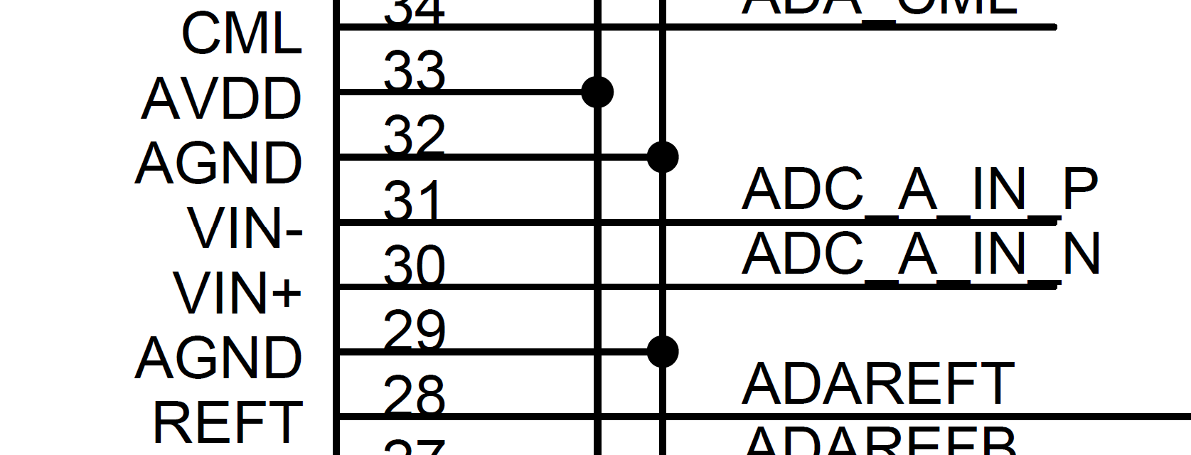
Fig. 26 Polarity inversion.#
BALUN circuit#
BALUN (balanced-unbalanced) is a circuit use to transform an unbalanced signal to a balanced one. Usually, an input series-resistance is used for impedance matching so that the output voltage corresponds to the input before the resistance (it is the double of the one in B+–B-)
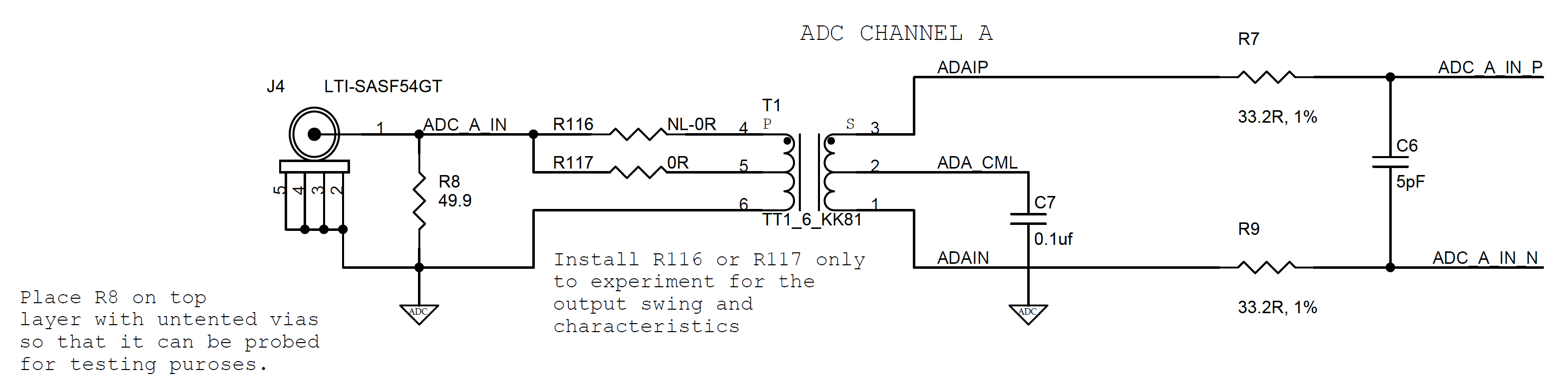
Fig. 27 BALUN circuit in the daughter board from the schematic.#
More info at this link from Digikey.
Resources#
Link to all the resources
zip file
DE4 schematics
DE4 manual
DE4 getting started
c
DCC schematics
DCC DAC5672
DCC AD9254