Diary 2024#
January 2024#
Went back to work on it after a long period dedicated to the lecture at UPS.
1st week of January - Found a (the) problem in the state machine. Regularization cannot be applied to jumpsets signals since two out of four are only an impulse, therefore it cannot be regularized. We might think to different variable that could be controlled/regularized. To discover this I simulated the controller with ModelSim feeding waveform from a PSIM simulation (directly vC and iC of the ADC).
2nd week of January - Try to set up a simulator for the dynamics of the converter. So far it seems good, I discovered of the priority of arithmetic vs logic operations. This took me several hours of trial and error among ModelSim, PSIM and MATLAB.
9 January - Simulation module for LLC is working, a module to transform the output to an ADC like is missing.
30 January - start to write the draft for a Transaction paper and lunch the discussion on it.
Other#
March - start to going back to work on the charger application using what Carlos has prepared on the comparison with different Quality factors.
1 March - the \(phi\)-control law (and possibly also the \(theta+phi\)) can be cast as checking where the trajectory in \(x\) (non-shifted coordinates) is in the phase-plane, without the need of the shift. This implies that just a state machine which ensures the right order (i.e. prevents to go back) should be enough.
12 March - start to put together the things used for the future TPIE paper
Long long break
During April, I mostly focus my self on the writing of the thesis. Trying to harmonize the mathematical description and modeling took more than expected.
May 2024#
3 May 2024 - Merge of the note on the design of the prototype on the thesis
— Back in TGN and at Campus Sescelades, Planta 4 —
5 May - Start of the 4-weeks period in Tarragona to try to ultimate the prototype. I’ve arrived in Tarragona pretty fast (6h), but with the managing of the trains a bit sketchy.
6 May - Going back to the work and discuss with Carlos. Try to find the state-machine that is working and then implement the control law in x-coordinates, which should be more robust. There are problems with keeping up the signal and at startup. The signal \(\sigma\rightarrow v_S\) seems delayed.
7 May - Checking for the delay: it is actually there, around 600ns. Using \(\phi<<1\) creates more glitching. I do not know the reason. The definition of the set in x-coordinates was inverse (1 is negative and 0 positive). It seems better by taking the zero zone as half plane. At least we cover the case phi=0. In the end, using regularization, the controller in working with the state-machine in \(x\)
8 May - Improve the code for controlling values, now it goes up and down, thanks to ChatGPT: tip -> it was enough to manually recognize a button without going through the posedge/negedge.
Characterization of the sensor for the current in the output of the rectifier: it takes a lot of time. Measure are done to first evaluate the curve of the sensor and then to link the sensed value to the digital value. When all the chain is known we can compensate for it and show a semi-exact representation.
The same thing is done for the voltage sensor.
The current sensor has an offset and it is pretty much linear.
Instead, the voltage sensor seems to have a slight distortion.
9 May - While testing the current sensor, the characteristic current-voltage remains constant; what does not remain constant in the HEX lecture in the FPGA. It changes every time… I have no idea of the reason. It has been a long day. The test for the output sensor have been done by connecting the power supply directly to the rectifier, without using the bridge. Many things have been done
on the current sensor, change the OPAMP from follower to differential: connect the ground to the Vref point. In this way we are removing the offset and we have a wider range for the current. With the current resistor we can read up to 20A more or less.
on the voltage sensor I decrease the range of the input by changing the resistor of the voltage divider from 120 to 180 Ohm. We can go up to 60V before the input of the ACPL reaches the limit value of 200mV.
input/output curves have been obtained.
voltage: it is linear, but the ACPL seems to have a gain of 4.65 instead of 8.2 (from datasheet). The slop of the line is more or less 3
current: now it is linear, without the differential-opamp it seems that the turn ratio N was 0.5 but indeed it is 1. The inclination of the interpolating line is more or less 15. Now, also the displays showing the decimal value are working. The wire connecting the blocks was not declared, but also I had a module doing the job
num2segthat was not used. We could tune in a finer way the sensor. Now it is not that bad, we have an error in the order of 0.2A and 2-7V (higher with higher voltage).
10 May - First thing in the morning… wake up late so that I can not go to the swimming pool :|. Apart from the jokes, I’ve connected back the H-bridge and all is still working. I had the \(22.8\;\Omega\) load connected, I’ve been able to go down until 500mA more or less at the output with \(\varphi=50\). We can clearly see that also at the resonance the waveform is no more sinusoidal since the quality factor is low. The open-loop version is at its final stage. I don’t think there is more work to do. All the control laws with \(\varphi\) are implemented in the \(x\)-plane and this enhanced the performance of the phase-shift modulation. There is a problem with the mixed control. We can clearly see that the input voltage is asymmetric. This is due to the fact that there is a bias in the current \(i_S\) that is read by the ADC. The reason in not clear since the other switch is correct. Moreover, check with the oscilloscope, the voltage at the exit of the signal transformer is good and in phase with the measured current. What is shifted, is the current after the \(49.9\;\Omega\) resistor. I tried to change the position of the resistor in the PCB and to disconnect the capacitor, but this had no effect.
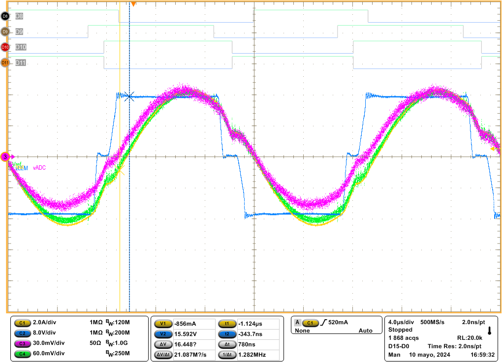
Fig. 17 Distortion in the tank current sensing. Current (yellow), voltage after the transformer (green), voltage after the 49.9Ohm or at the input of the ADC card (purple).#
11 May - Working in the morning and “climbing” with Ramon and Julia in the afternoon at La Mussara, sector Can Pistola.
12 May - Working a bit and then bike ride in the afternoon. 75km long along the coast until Creixell and after towards the inside until Montserri and back through el Catller.
13 May - Try to set up the modules for the closed-loop. I spent much of the morning looking on ways to code a PI with fixed point numbers (i.e. integers). Carlos suggested a nice book from Luca Corradini et al. “Digital Control of High-Frequency Switched-Mode Power Converters”, which contains useful tips for the implementation. The biggest problem is the scaling having to use only integers numbers. Moreover, it is not yet clear how to design formally the closed-loop. Apart from this, I’ve cleaned the TOP file and incorporate the debug on the 7 display into a module (the RTL view is cleaner). The objective is to regulate the current up to 0.1A, but the PI is running with mA resolution to have a margin with the operations and avoid the numbers to be clamped to zero. We work with 32bit integers (probably this could be reduced). In the end, the converter starts oscillating but it will stop since the control becomes \(\varphi=\pi/2\). The objective will be to try to understand why it is going to saturate in that direction. We can see the value of \(\varphi\) through the digital probe.
14 May - Starting by cleaning up a bit the TOP and debugging the PI. A problem stands in the saturation which is clamping positive values to the maximum and not the minimum.
Nice tutorial on operators https://documentation-rp-test.readthedocs.io/en/latest/tutorfpga04.html.
I’m spending a lot of time in debugging the saturation…
In the end, it is working by restraining the value of phi to 7-bit (64 max), which is a kind of brute force saturation.
I’ve tested the saturation block alone and they are working fine.
In the end, I make it work by cutting down the computed valued of \(phi\) to 8bit=sign+7bit. In my opinion it should work also with the 32 bit, but for some reasons it was always limiting to the maximum value. Probably there were some bit that were given problem, so that the phi after the PI was larger than 90, but due to some other reason, and the most useful information was standing in the first bits.
Final consideration: it is WORKING. Strange but true, now I need to show how to compute the gains based on some design specification.

Fig. 18 Output current (green) that stabilizes to different set-points changed with the buttons. In yellow the input current.#
15 May - An archive copy of the code has been created. The converter starts to work badly over some level of input voltage, essentially there is noise entering the tank sensing. Also, working with high currents, heat up a lot the converter (resonant capacitor and inductor, load, and cables). It seems that the sensing range for the tank is respected, anyway it starts doing nap-nap (n’importe quoi ×2). I’m trying to understand the behavior of the tank+filter in open loop in order to have a bare model of the system. Yet, I’m not able to remember why the behavior is asymmetric with a resistive load. Ok, the damping in the resonant tank changes (\(R_{eq}\)), but not the one in the filter. Probably we can see them as two separated blocks:
the tank with its second order response (LLC is 3rd, answer to sinusoidal should be 2nd…)
the filter with its second order LPF characteristic. Essentially, the tank is modulating the current envelope, while the filter is smoothing this envelope.
When increasing the input voltage, the resonant tank start glitching (switching \(\sigma\) when not expected). I tried to extend the regularization time in the control: no difference. For the asymmetry for low \(\varphi\) the problem is coming from the current sensing that is introducing an asymmetric scaling. Trying to solve this by connecting two resistors directly to the output of the signal transformer (there are four 49.9Ohm resistors that connect the transformer to the ADC): this hasn’t solved the problem, even, it seems to amplify more the noise. Just some extra work since the layout was more complicated than expected.
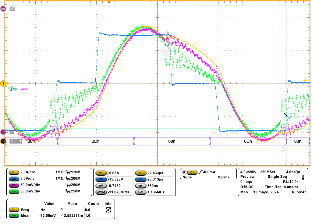
Fig. 19 Distortion in the tank current sensing, still there after the layout changes. Current (yellow), voltage after the transformer (purple), voltage after the 49.9Ohm or at the input of the ADC card (green).#
In the night I fixed the problem with the simulation analysis. There was a wrong consideration in the DSP_analysis.m (loc is empty if there is no peak); then there was an error in the implementation of \(\theta\)-control law in the \(x\)-plane (it can actually re-cross the line if there is no shift, so the jump set definition must be different). Fixed the integration step to 10ns, 5ns for \(\theta\) in the \(z\)-plane since needs more precision. Moreover, having a variable integration step was giving problem with the FFT.
Finally, I don’t see the advantage of the control law in the \(z\)-plane, the one in the \(x\) plane from Ricardo seems better (lower frequency peak and nicer input-output relation).
16 May - Start to stare at the electronic load. The behavior with a battery as a load is pretty different, a higher output current can be reached with higher values of \(\varphi\). I’m trying to make the code more robust by adding an over-voltage protection and a restart when it turns OFF when not desired. End: OverVoltage works, the RESTART does not (it is more complicated since it could make the RESET signal remaining low causing the converter to stay OFF).
In the afternoon I tried to connect the electronic load (EL). More or less it works, but it is hard to turn on the converter due to the Over Voltage protection. Setup: EL at 20V and Vg=24V. Essentially, at the turn-ON the EL voltage goes higher than the selected 20V, specifically higher than the OV limit, causing the converter to shut down. What we can see from the oscilloscope is that the voltage at the output is rising and then it goes down. TO overcome the protection problem, we can turn on the converter in OL with \(\varphi=50\), then we can go down with \(\varphi\) until we match a current value and the reference, at that point we switch to the CL control. This works and then we can regulate from 0.5A to 5A. If we remove the OV protection, the converter starts “normally” and reaches the desired operating point. But, what is interesting is the behavior at the turning-ON: Vout rises and then drops, and it does this few times (~5) in a triangular fashion, until it stabilize to the set Vout. In the meanwhile, the current drained by the load has spikes, they disappear once the voltage is stable and then the current converges towards the desired point.
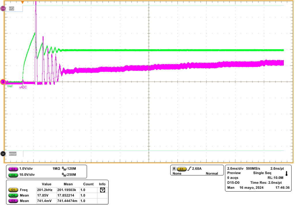
Fig. 20 Current (purple) and voltage (green) at the electronic load during the startup phase.#
17 May - Clean the chapter of the thesis on the design i he descansat. In the afternoon I’ve done some measurements for different value of the output voltage, so far they seem to track what expected. Anyway, the converter is working with 24V and not with the 48V for which it was designed. I need to check the proper definition for ZVS and ZCS, mostly ZCS to check if it is happening. Below, the curves obtained from the measurements. They match the one that Carlos has in the presentation.
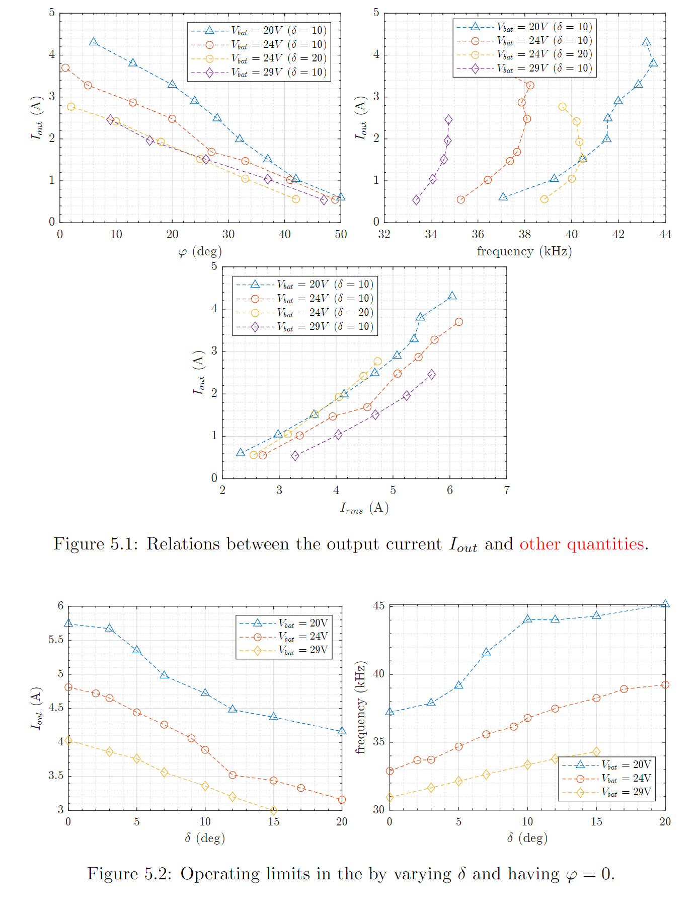
Fig. 21 Point measure with the oscilloscope.#
18 May - Work from home and groceries. Clean up the section on the resonant tank sensing.
19 May - Flea market and working from home. I’ve created a PSIM simulation that should work as reference for theoretical behavior of the prototype. The antiwind-up behavior has been added and there was a problem with the scaling, i.e., Kaw is much higher than Ki Kp since the error scale is higher than the phi scale.
20 May - The converter decided that it is not the day to work. It starts with low amplitude and then we can move it to a working point with higher amplitude (lower phi); but if we start it directly with low phi it starts glitching and making noise (music). A reason might be that it experienced high voltage since I turn it ON with the electronic load in standby. The output was saying 100 something Volts. But, if I run it in open-loop it is working without problem, even reaching phi equal to 80deg. Ok, I’m going out crazy. Simulations in PSIM result with a higher frequency than expected, around 100kHz (the block to compute the frequency had an error, it was not necessary to divide by 2). While, the prototype is working at the expected frequency. The reasons are so far unknown.
Then, why is the converter turning OFF when I use the CL but not when it is in open loop? I’m testing at 24V. For some reasons, in OL the voltage \(v_C\) is within the forecast bound. In CL, it is overflowing it, causing the ADC to go in overflow. One way it to clip the value in the FPGA by managing the overflow bits, another way is to change the sensing circuit. In the end I change the resistor Rpv1, the one that steps-down the voltage on the tank side, from 4.8kOhm to 8.2kOhm. I’ve also added a piece of code that should manage values out of the range, I think the problem was meanly related to the fact that we are inverting the number, and the negative overflow 100000 corresponds to the same, which then was read as a number with inverse polarity.
Then, the open-loop works smoothly. The closed-loop also considering a resistor as load. It seems that the antiwind-up in this case is not working since when we are near to phi=0 it stops instead of keeping phi=0.
With the electronic load is more problematic. First, there is a transient behavior at the beginning that is creating high current and voltage in the resonant tank with low-frequency (around 20kHz). Then, the converter may stabilize to a point but it can also turn OFF.
I’m so stupid or so fucked up, right now idk, that I copied the PSIM simulation from the old folder without remembering that I was working on another version in the folder 2024_OBC. So there was still the error on the diodes’ capacitance.
Simulation in now working in
THESIS_ALLPI with AW is working in simulation
The range for \(v_C\) could still be too small for a full rated power
21 May - Heures au telephone avec les services françaises qui te mis en attent. In the end is herpes and I have to rest. So, I’m working from the apartment on the thesis and I’ve started using circuitikz, easier than expected once you know how to use the coordinates.
22 May - Another day working from home
Went to check if the controller it is working. Still, it has problems and I haven’t solved much. I feel that the time start to be limited and this might be stressing.
23 May - Back in the lab with the same problems.The controller in CL is not able to stay ON for small references, while for larger one it fails when phi is near zero. The converter is glitching and this is due to the rapid changes in phi, I try to solve this by filtering the estimated current. Today I’ve done few changes that, I think, have a major impact:
Remove the inc=2 if \(\varphi=0\), so that, it always goes through \(\sigma=0\). This solved the problem that was arising in the case \(\varphi\) was going to zero while \(\sigma=0\), this implied that \(\sigma\) stayed at zero for the whole time.
In the generation of the clock signal for the state machine, look two steps back to reset the clock down to zero (¡I don’t know if it might be dangerous!).
Introduce a saturation module that by construction has the lower limit at zero. This might be not necessary, but it is safer since the behavior is more predictable to me.
Add a low-pass filter on 4 sample on Ibat expressed in mA. This improved the behavior with small amplitudes by making it more robust. The oscillations in \(\varphi\) were causing the converter to shut-down.
Try to fix the regularization block. I think that it was not working properly. It needs more testing. The converter without the AW is working super fine, the problem is that it is going in overflow after some time. The AW is making the behavior at the limit worst, as if \(\varphi\) is oscillating.
For the AW I’ve done several tests with different gains but it is not working. PSIM simulation is fine but FPGA does not agree on this.
I’m trying in simulation to see how it will behave a controller just working in the frequency modulation scenario (change only \(\delta\)). The input/output characteristic is a bit strange and in a certain range it has a huge ripple.
24 May - Debugging and debugging again as style of life. The regularization seems to work.
Then, after several trials, the PI block need to have signed number. The reason: operation >>> (arithmetic shift) adds trailing 1 or 0. But it adds 0 iff the MSB is 1 and the register (maybe also wire) is declared signed. Otherwise, it is always adding 0 making the number becoming positive.
I finish the day by taking measurements of the quantity in the resonant tank and in the sensing.
We should try to put a big capacitor in parallel with the electronic load to see if the behavior is better.
27 May - Let the last week to start. Both electronic loads are out :o, non really, one seems out, the other has problem in regulating the output voltage, probably the two controllers are clashing with each other and this results in an oscillating behavior in the electronic load. David might help me tomorrow in attaching a real battery and see what is the real behavior.
I’m going to improve the TOP_open_loop so that I can do the tests.
After a long the day the result is: improved open-loop code with more options. I solved some compatibility problems and done some updates after new insights from the closed-loop. Now, what the OL can do is:
by acting on
sw[2:1]we can choose the controller00 phi + delta
01 theta in z-plane (improved version with regularization)
10 theta in x-plane (run on mixed control by changing delta)
11 phi in x
the angles phi and theta are changed with the buttons [1], [2] and reset with [0], delta with [3] and reset with [CPU_RESET]
Anyway, the offset/distortion on the current measurements is still present. Sometimes it seems not important other yes…
On the closed-loop. The original electronic load is officially dead, the older one is still interacting in a bad way. The last possibility is to use a real battery, another temporary solution might be to use a big capacitor (mF) in parallel with the EL.
In the night I have clean the file that calculates the gain for the measurements and measure the gains from the capture. Now there are csv files with the measurements and MATLAB script for the interpolation. I aim to draw the plot with Tikz.
28 May - Update the gain for the controller by characterizing the sensing: mu_vC=160, mu_iC=90, mu_Vg=312000[24V] or 624000[48V]. Today is measure day. I’ve taken several measurements to have points for the open-loop control laws. There is the distortion/offset in the current sensing that is moving the system from the predicted behavior when amplitudes are small.
Then, thanks to David, we attached the converter to a 48V battery cluster, and it is working! We can control down to 200/500mA, up to 6.5A (limited by the resonant tank sensing circuit).
I create the MATLAB code to analyze the data from the oscilloscope in open-loop.
29 May - I’m particularly tired today, idkw (fatigué, cansado, cansat, stanco). The efficiency is low today, I’m probably getting sick again.
Anyway, I took several operating points by measuring directly on the oscilloscope and note the values on a *.csv file.
The workflow is: measure with 48V; increase to 52V; and then go down to 38/10V. Otherwise, it will take a lot of time to charge back the batteries.
What has been measure is: 1st harmonic value of vS and vT, input rms current, frequency, and output current.
Definitely I was not feeling good that day.
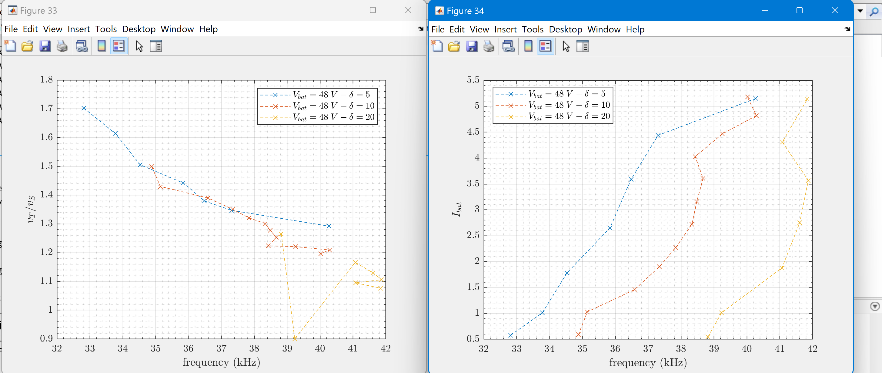
Fig. 22 Operating point of the converter with a battery attached to it#
30 May - Go back to the lab to fix some last measurements. Mainly OL measurements to complete the one I took before. Dead-time used for the measure is 600ns. NOTE: measurements with 4R3, delta=10 and variable might have the wrong measure of vS. I’ve taken capture for the ZVS. Some for the ZCS are missing.
31 May - last day in the lab, crowded by measurements’ duty ;). I tried to take capture of several things that I might need: ZCS with the battery as a load, limit cycles with battery and with resistors, and closed-loop response. I have also taken photos of the prototype.
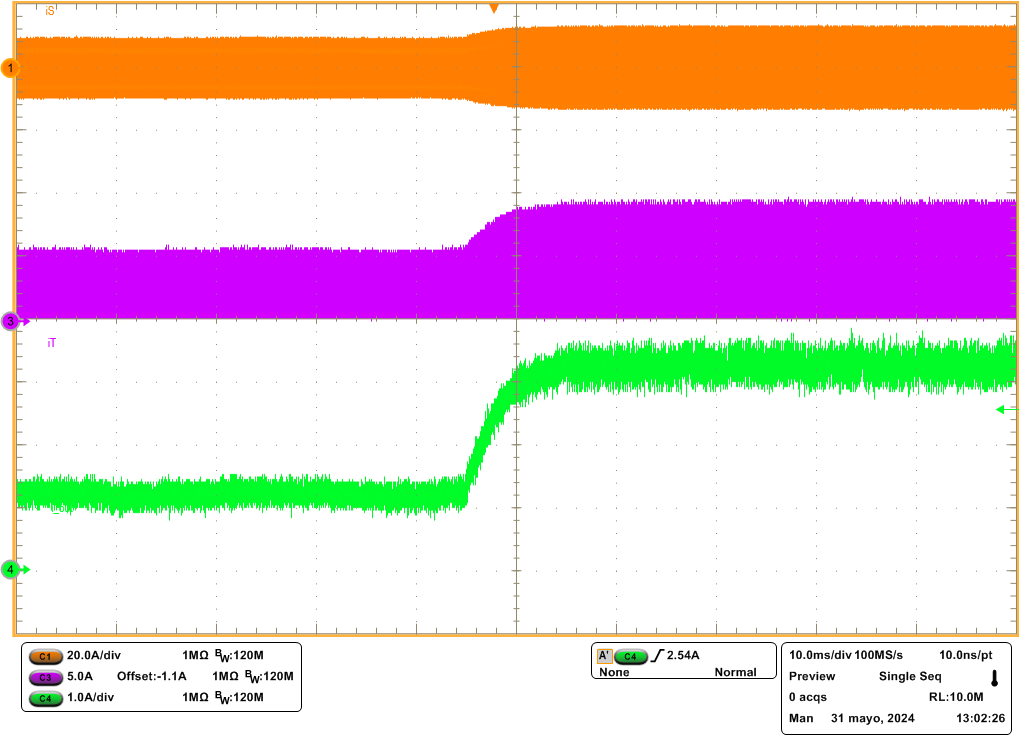
Fig. 23 Closed-loop response#
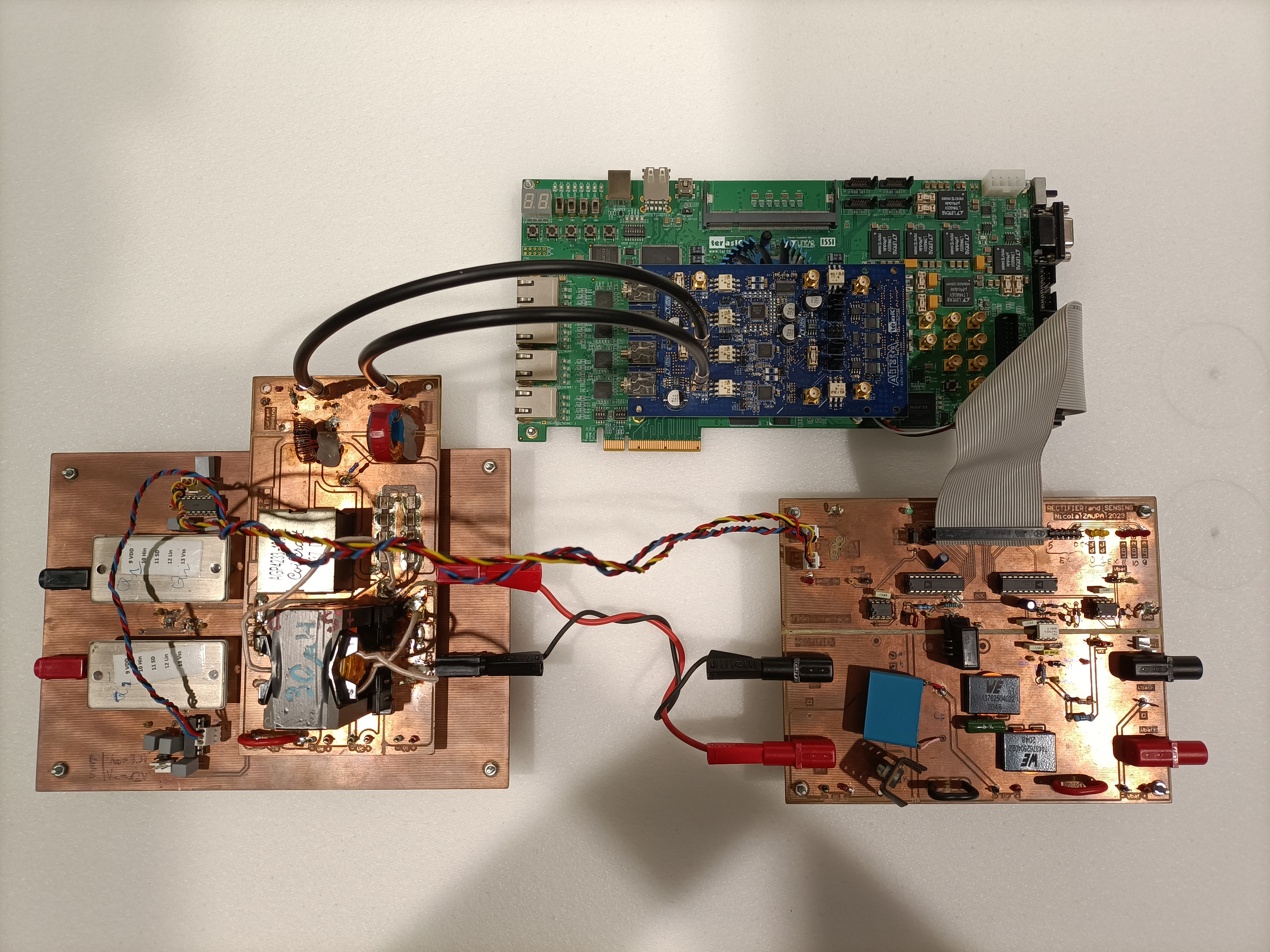
Fig. 24 Prototype on 31st May 2024#