Sensing#
The current and the voltage on the capacitor \(C_r\) are measured in order to close the loop and ensure the oscillation. Two sensing circuits are used to measure these quantities. Thanks to the use of signal transformer, the resonant tank is galvanically isolated from the sensing output, i.e. the FPGA1. The transformer design procedure is described in Signal Transformers.
Every sensing circuit must have the least influence possible on the resonant tank.
The output of the transformers need to be interfaced with a BALUN circuit, which is embedded in the acquisition card. Essentially, we can see it as a \(49.9\;\Omega\) resistor in parallel with the output of the sensing circuit. Remember that, the voltage that is read by the ADC is the double of the output, i.e. apart from filtering behavior, it corresponds to the voltage out of the transformer. (the two \(49.9\;\Omega\) resistors are dividing in half the voltage, which is the doubled by the BALUN circuit thanks to a transformer). The limit voltage is \(0.5\;V\).
Practically, every sensing stage is connected with a SMA connector via a coaxial cable to the ADC board.
Current Sensing#
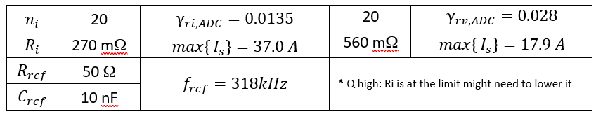
The capacitor current corresponds to the input current of the resonant tank. A current-transformer is used to sense it and to ensure isolation. The primary current is reduced at the secondary according to the transformation ratio \(1:n_i\), which is then transformed to a voltage thanks to the resistor \(R_i\). The best choice is to have the least number of windings at the primary, so that the magnetizing inductance is negligible with respect to the resonant inductance \(L_r\).
The static equation relating input current \(i_S\) and output voltage \(v_{R_i}\) is
where the approximation is valid in the case \(R_i\ll100\Omega\). The static relation between the current and the ADC value is the following
The dissipated (AC) power on \(R_i\) is approximately \(P_{R_i}\approx \frac{R_i}{n_i^2}\frac{I_{S}^2}{2} \), where \(I_{S}\) is the peak value (\(i_S\) is an AC signal so we should consider the RMS value for the power or the peak divided by \(\sqrt{2}\)).
The equivalent resistance at the primary side is: \(R_{T1,eq}=\frac{R_i}{n_i^2}\).
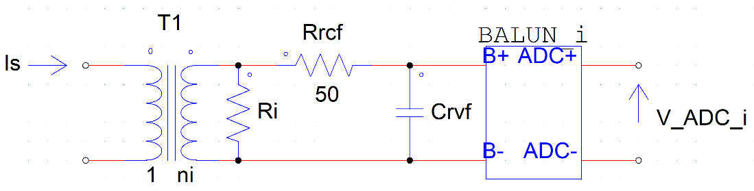
Fig. 5 Current sensing circuit#
A transfer function can be written between input and output:
Where \(V_{ADC}\) indicates the voltage that is than transformed to binary code (double of the voltage on the filter capacitor).
The output of \(T_1\) is connected to a SMA connector through a low pass filter with cut-off frequency \(f_{rcf}=\frac{1}{\pi\ R_{rcf}C_{rcf}}\). \(R_{rcf}=49.9\Omega\) for impedance matching with the input stage of the ADC.
Note
Small interface to calculate de maximum current from ADC data and values of the components.
Voltage Sensing#
After have experience some problem with high voltage sensing, we can generalize the acquisition chain as:
capacitor grid reducing of an integer factor. e.g. \(3\times3\) grid (\(9\) capacitors) reduces of a factor \(3\). It is suggested to keep it symmetric with an odd number. We might think of some other configurations. The important is that the equivalent capacitance is \(C_r\) (does not waste power);
voltage divider with 3 resistors to attenuate the voltage (waste power);
signal transformer: connected to the central resistor, step down the voltage and ensure galvanic isolation.
Warning
These considerations are important for high voltage and, indeed, they haven’t been tested.
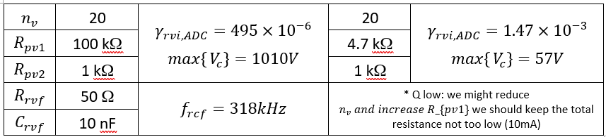
The voltage is initially attenuated by a grid of capacitors (the resonant ones) of a factor \(n_c\), then by a voltage divider by a factor \(\frac{R_{pv2}}{R_{pv1}+R_{pv2}+R_{pv3}}\), which is then attenuated by a signal transformer with transformation ratio \(n_v:1\). Therefore, we have that the voltage read by the ADC corresponds to
Equivalent resistance at the primary is \(R_{T2,eq}=2R_{rvf}n_v^2\), and we need to have that \(R_{pv2}\ll R_{T2,eq}\).
The static relation between the voltage and the ADC value is the following
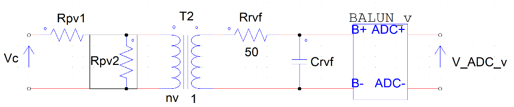
Fig. 6 Voltage sensing circuit#
A transfer function can be written between input and output:
Where \(V_{ADC}\) indicates the voltage that is than transformed to binary code (double of the voltage on the filter capacitor).
Then, the output of \(T_2\) is connected to a SMA connector through a low pass filter with cut-off frequency \(f_{rvf}=\frac{1}{\pi\ R_{rvf}C_{rvf}}\). \(R_{rvf}=49.9\Omega\) for impedance matching with the input stage of the ADC.
Caution
It’s really import to consider the magnetizing inductance of the signal transformer. Its effect should be negligible and to evaluate this we can consider the equivalent impedance at the resonance frequency. Essentially, \(Z_{eq} // R_{T2,eq}\) must be higher that \(R_{pv2}\).
Interaction with the FPGA#
The gain of the ADC, considering the voltage before the impedance matching resistor, is equivalent to
where \(0.5\) is the voltage range of the ADC.
Once we have the measurements, for the control law we need to scale them in order to have values that allows computing a scaled version of the state of the system \((z_1,z_2)\). First of all, for all states, we consider a common scaling gain \(k_{com}\). This is useful to increase the precision since the operations are done with integers numbers. It should by high enough to make the gains greater than 1, and not too high in order to avoid overflow. The higher the better the precision.
For the current related state, we have that \(z_2=\frac{1}{V_g}\sqrt{\frac{L_r}{C_r}}i_S\). For the voltage related state, we have that \(z_1=\frac{v_C}{V_g}-\sigma\). We scaled both y \(V_g\) and we also need to scale both \(v_C\) and \(\sigma\). The resulting gains are:
On \(V_g\) scaling
Remark that all the scaling with respect to \(V_g\) have been removed, i.e. they have been incorporated by \(\sigma\). This is possible since for the control law we can use any scaled version (by the same factor) of the states \((z_1,z_2)\). Another way to see it is that they have been incorporated by \(k_{com}\).
Caution
\(k_{com}\) should avoid the overflow situation. Check it analytically is a bit hard. One conservative possibility is to take the worst scenario and use that to limit it. Another way is simulate the behavior, to this end there is a PSIM simulation that implements this behavior and can be used to check limits.
EXTRA#
need to understand where and how to put this
\(n_i\) |
20 |
\(\gamma_{ri,ADC}=0.0135\) |
\(R_i\) |
270 \(mΩ\) |
\(\max\{I_s\}=37.0\ A\) |
| ni | 20 | γri, ADC = 0.0135 max {Is} = 37.0 A |
20 | γrv, ADC = 0.028 max {Is} = 17.9 A |
|---|---|---|---|---|
| Ri | 270 mΩ | 560 mΩ | ||
| Rrcf | 49.9 Ω | frcf = 318kHz | * Q high: Ri is at the limit might need to lower it | |
| Crcf | 10 nF | |||
| nv | 20 | γrvi, ADC = 495 × 10−6 max {Vc} = 1010V |
20 | γrvi, ADC = 1.47 × 10⁻³ max {Vc} = 57V |
|---|---|---|---|---|
| Rpv1 | 100 kΩ | 4.7 kΩ | ||
| Rpv2 | 1 kΩ | 1 kΩ | ||
| Rrvf | 49.9 Ω | frcf = 318kHz | * Q low: we might reduce nv and increase R_{pv1} we should keep the total resistance not too low (10mA) | |
| Crvf | 10 nF | |||