ADCs#
The last stage for the sensing is in an ADC. The AD78221 is used, it is a 8-bit half-flash ADC. It has a conversion time of 420ns and the output bits are in parallel. It can be supplied with 3V or 5V, with respectively input range of 2Vpp or 2.5Vpp.
The ground is shared with the FPGA and it is different from the one of the battery by design choice.
LINK to PDF file Moon converter.
Pin connections:
To GND
VMID (through 100nF cap)
VREF (through 100nF cap)
AGND
DGND
CS
RD with EOC to FPGA with 1k resistor
CONVST to FPGA with 1k resistor
PD to VDD
VDD with bypass (through 100nF , 10uF)
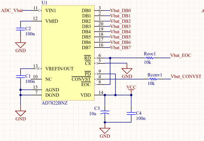
Fig. 16 Circuit for the ADC#