Sensing#
We need to sense DC values to close the loop, mainly the current. The voltage is used more for a safety reason.
The power supply for the electronics in the sensing part (ADCs + OPA) can be taken from the FPGA, which has 3.3V and 5V pins on the GPIO 40-pin socket.
The requirement behind this sensing stage is to keep the ground of the battery separated from the one of the FPGA. To this end, we aim at using isolated sensors. Therefore, for the current a Hall effect sensor is used; while, for the voltage an isolated operational amplifier is used. Outputs of the sensors are actively filter with operational amplifiers (LPF) to reduce the noise. Finally, ADCs are used to transform the signals in digital ones, directly connected to the FPGA with a parallel interface.
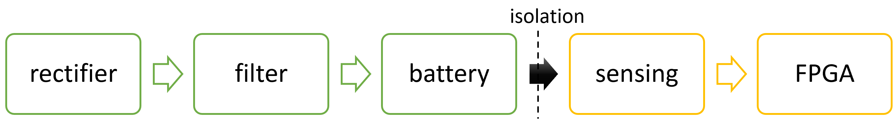
Fig. 9 Scheme of the main stages in the circuit#
sensor range must be compatible with the measurement to be done
sensor output must be compatible with the ADC input
Battery Current Sensing#
For the current, there are two isolated options:
Hall-effect sensor;
Shunt resistor with isolated op-amp. One main difference is that the Hall-sensor does not require power supply in the input side, whereas the isolated opamp need it to work.
The final choice is for a Hall effect sensor. One common possibility comes from the LEM family, in particular the HO series. They are distinguished by the current range (6/10/25) and the supply voltage in the output side (3.3/5 V).
The output voltage depends on: a fixed gain \(\gamma\), the number of turns \(N\), and an offset defined by \(V_{\text{ref}}\), which corresponds to half of the supply voltage.
Note
Based on the sensor shape, the current can be sensed with:
a wire wrapped around the hole and the number of turns \(N\) is free;
the pins, every couple is a wind, therefore they can be connected in parallel, i.e. \(N=1\); or following a configuration to reach up to \(N=3\).
The general simplified input-output relation is the following
At \(I_P=0\) the output voltage is \(V_{out}=V_{ref}+V_{OE}\), with \(V_{\text{OE}} \in \lbrack -10,10\rbrack\text{mV}\).
Some data from the series
series |
\(+U_c\) |
\(V_{ref}\) |
\(\gamma\) |
input range |
nominal rms |
output range \(|V_{out}-V_{ref}|\) |
|---|---|---|---|---|---|---|
HO 6-P |
\(5\;V\) |
\(2.5\;V\) |
\(100\;mV/A\) |
\(\pm20\;A\) |
\(6\;A\) |
\(\pm2\;V\) |
HO 10-P |
\(5\;V\) |
\(2.5\;V\) |
\(80\;mV/A\) |
\(\pm25\;A\) |
\(10\;A\) |
\(\pm2\;V\) |
HO 25-P |
\(5\;V\) |
\(2.5\;V\) |
\(32\;mV/A\) |
\(\pm62.5\;A\) |
\(25\;A\) |
\(\pm2\;V\) |
HO 6-P/SP33 |
\(3.3\;V\) |
\(1.65\;V\) |
\(76.67\;mV/A\) |
\(\pm20\;A\) |
\(6\;A\) |
\(\pm1.15\;V\) |
HO 10-P/SP33 |
\(3.3\;V\) |
\(1.65\;V\) |
\(46\;mV/A\) |
\(\pm25\;A\) |
\(10\;A\) |
\(\pm1.15\;V\) |
HO 25-P/SP33 |
\(3.3\;V\) |
\(1.65\;V\) |
\(18.4\;mV/A\) |
\(\pm62.5\;A\) |
\(25\;A\) |
\(\pm1.15\;V\) |
The maximum current consumption is of 25 mA.
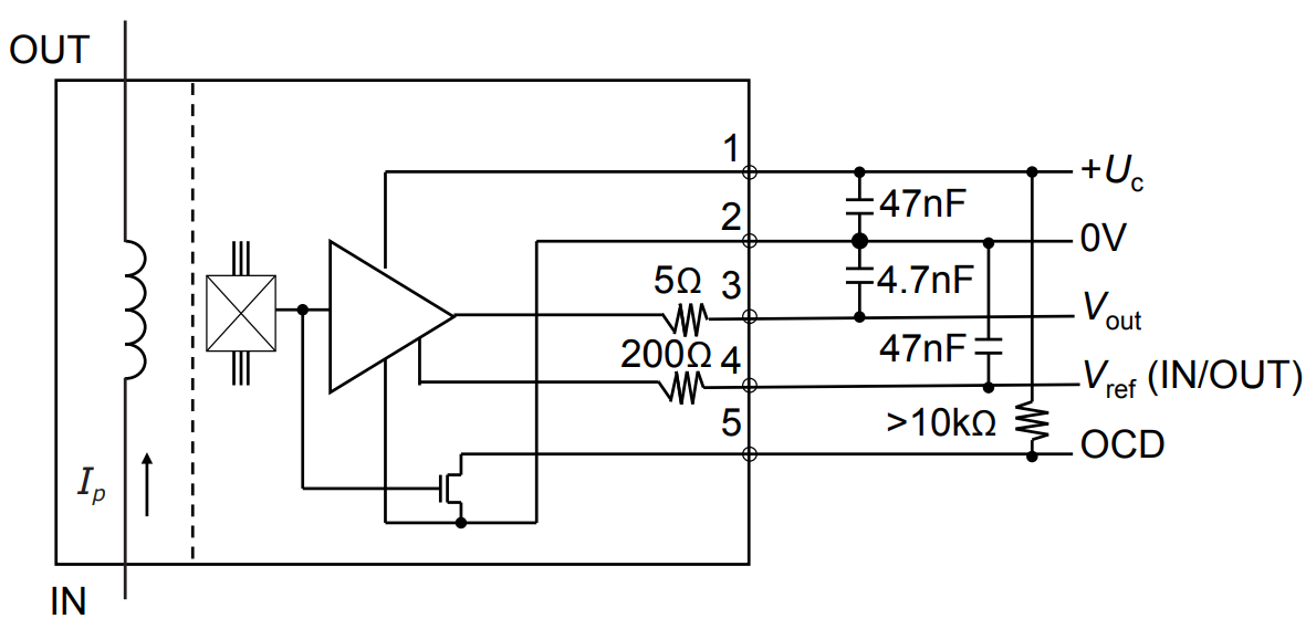
Fig. 10 Operational principle of HO x-P#
More complete model from the datasheet:
The output of the sensor is then conditioned in order to attenuate the amplitude and filter it with a LPF. There is a first stage reducing and filtering, then the opamp could be use either to as a voltage follower or an amplifier (gain>1).
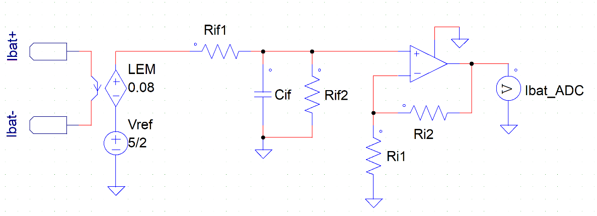
Fig. 11 Current sensing stage#
The LPF cut-off frequency is \(f_{i} = \frac{1}{2\pi\left( R_{if1}\text{//}R_{if2} \right)C_{\text{if}}}\) with DC gain \(\frac{R_{if2}}{R_{if1} + R_{if2}}\) and the gain of the op amp is \(1 + \frac{R_{i2}}{R_{i1}}\)
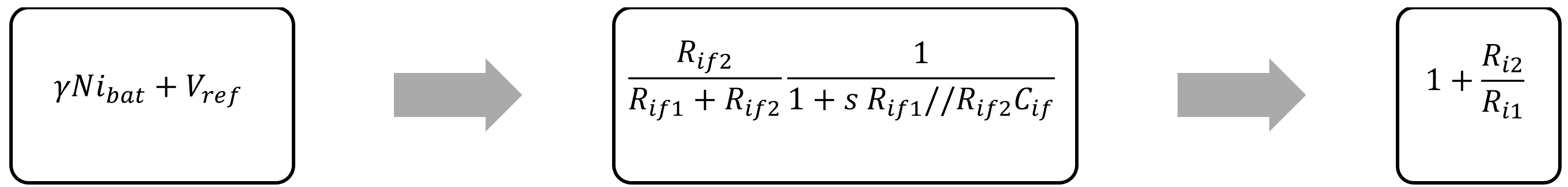
Fig. 12 gain and filter chain under approximation#
Battery Voltage Sensing#
As for the current, we want to keep the measurement isolated. Therefore, the sensing of the battery voltage is done with an isolated op amp. A typical series used at this end is the ACPL from Avago Technologies / BROADCOM®.
The voltage is initially reduced with a voltage divider and it is filtered with a LPF. The sensor is the ACPL-790B-000E, which has a fix gain of 8.2 with differential input and output. The signal is then referenced to ground with a differential op amp, which includes another LPF stage.
ACPL-790B-000E |
Isolated opamp with \(\pm 0.5\%\) High Gain Accuracy with fixed gain \(\times8.2\). Supply voltage: from 3V to 5.5V for the output side; 5V for the input side. 200kHz bandwidth. DIP-8 package. Input range \(V_{in+}\Leftrightarrow\pm\) 200mV recommended. Power consumption: 18.5mA on the input side and 12mA on the output side. |
Warning
The ACPL has an input resistance of 27 kΩ. Therefore, we cannot threat it as a standard high-impedance input operational amplifier.
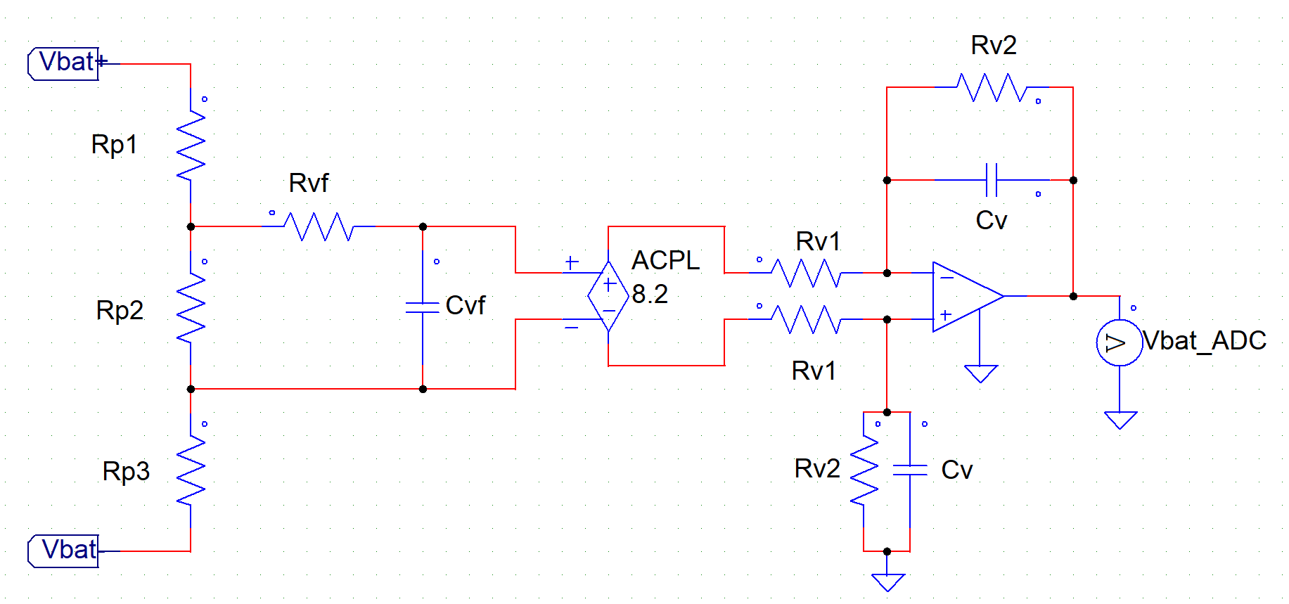
Fig. 13 Voltage sensing stage#
In ideal condition (almost constant voltage on \(R_{p2}\)), the input differential voltage corresponds to \(v_{\text{in}} = \frac{R_{p2}}{R_{p1} + R_{p2}}v_{\text{bat}}\) and the cut-off frequency of the input filter is \(f_{\text{vi}} = \frac{1}{2\pi R_{\text{vf}}C_{\text{vf}}}\). We also need \(R_{\text{vf}} \gg R_{p2}\) to have a “simplified” version of the cut-off frequency
Full transfer function \(V_{\text{bat}} \rightarrow V_{\text{in}}\) is \(H(s) = \frac{R_{p2}}{R_{p1} + R_{p2}}\frac{1}{1 + s\left( R_{\text{vf}} + \frac{R_{p2}R_{p1}}{R_{p1} + R_{p2}} \right)C_{\text{vf}}}\)
the expression with the ACPL input impedance can be added
Take care that the input to the differential opamp has to have an amplitude less than 200mV.
The final op amp has a static gain of \(\frac{R_{v2}}{R_{v1}}\) and a cut-off frequency of \(f_{\text{vo}} = \frac{1}{2\pi R_{v2}C_{v}}\).
The total chain gain is: \(\gamma_{v_{\text{bat}}} = \frac{R_{p2}}{R_{p1} + R_{p2}}8.2\frac{R_{v2}}{R_{v1}}\ \) with two cut-off frequency for a LPF.
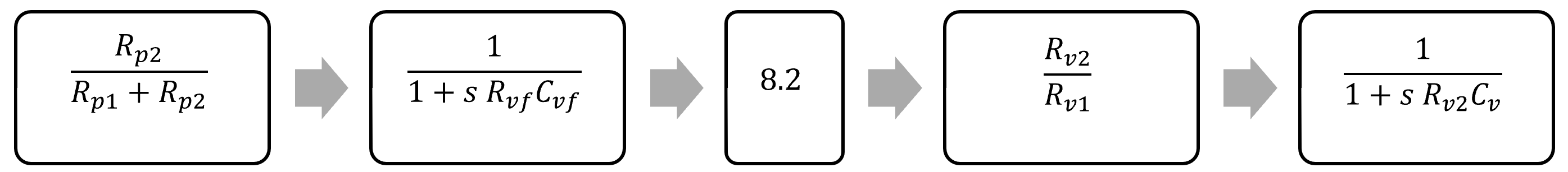
Fig. 14 gain and filter chain under approximation#
ACPL supply#
The voltage sensor needs to be powered from both sides. On the battery side it requires a 5V supply. To ensure it we can take the battery voltage and stabilize it through a linear regulator. We need to consider that the drop voltage will be high, i.e. we are reducing to 5V and input voltage of about 60V. One option that is able to bear this input voltage is the ZXTR2105FF, which allows a maximum input voltage of 60V. Bypass capacitors of 1uf and 10uF are suggested, 1uF in input highly suggested with high input voltage. Are these capacitors available in SMD format?
For flexibility, a choice between battery voltage and external supply is possible through a jumper.
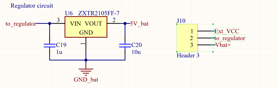
Fig. 15 5V linear voltage regulator on the battery side#